Something fundamental changed in the architecture of computing between 2022 and 2026. Not incrementally — not the kind of improvement that makes next year's laptop feel slightly faster — but structurally. The chips being manufactured today are not faster versions of what existed before. They are different kinds of machines, built for a different kind of work. And the consequences of that difference are cascading through every field where artificial intelligence creates value.
The catalyst was a realization that spread from research labs to boardrooms to government ministries: that the computational demands of modern AI — training large neural networks, running them at scale, deploying them at the edge — bore almost no resemblance to the workloads that decades of processor design had optimized for. General-purpose computing had hit its ceiling for these tasks. The only path forward was purpose-built silicon.
Why This Chip Cycle Is Unlike Any Before It
Every major computing era has been defined by a corresponding chip architecture. The personal computer era ran on scalar processors executing sequential instruction streams. The smartphone era depended on ARM-based designs that prioritized power efficiency. The AI era demands something categorically different: massive parallel compute engines capable of performing billions of simultaneous multiply-accumulate operations — the mathematical primitive underlying every neural network.

First: the improvement is exponential, not incremental. When you chart the performance of AI-optimized chips across consecutive generations, the curve bends sharply upward. Each generation delivers not 20–30% more capability but 3–5× improvement in AI-relevant workloads. The compounding effect of several such cycles is staggering.
Second: demand is structurally unlimited. Every improvement in AI capability generates immediate appetite for more compute to push the frontier further. The organizations racing to build the most capable models have no visible saturation point — better chips produce better models, which reveal new capability gaps, which require even better chips. The feedback loop has no natural ceiling.
Third: the chokepoints are geographically concentrated. Advanced photolithography equipment, leading-edge fabrication capacity, and specialized memory — the three pillars of AI chip production — are concentrated in a handful of companies and geographies. This has elevated semiconductor strategy to the top of national security agendas in ways not seen since atomic-era technologies.
Traditional processors execute instructions one at a time — optimized for complex, varied tasks requiring flexible control flow. AI processors execute thousands or millions of simpler operations simultaneously, optimized for the matrix multiplications and vector operations that underlie every neural network. As AI architectures have converged on transformer models, chips have grown even more specialized — including dedicated tensor computation units, on-chip high-bandwidth memory hierarchies, and communication fabrics that treat inter-chip data movement as a first-class design concern.
The Architecture Landscape: What Separates Leaders from Followers
The AI processor market is not a simple competition between a few large companies. It is a complex ecosystem of incumbents, challengers, hyperscaler custom designs, and architectural experimenters — each occupying distinct niches in a rapidly evolving landscape.
-
01
High-Performance Training Accelerators
The most demanding segment — chips designed to train frontier AI models from scratch across tens of thousands of parallel compute units. These systems require enormous memory bandwidth, ultra-low-latency inter-chip communication, and extremely high floating-point throughput. The organizations that own this segment effectively set the performance ceiling for all of AI research.
-
02
Inference-Optimized Processors
Running a trained model efficiently at scale is a different challenge from training it. Inference processors prioritize throughput-per-watt and latency-per-query. As AI deployment scales from millions to billions of requests, the economics of inference silicon become the dominant cost variable — purpose-built inference chips can dramatically outperform general-purpose accelerators for production workloads.
-
03
Hyperscaler Custom Silicon
The largest technology companies have developed their own AI chips tailored precisely to their specific model architectures and infrastructure. Custom silicon offers efficiency advantages unavailable from external vendors, plus supply chain independence. Industry projections suggest custom hyperscaler silicon will account for 30–40% of total AI compute capacity within the next two years.
-
04
Edge and On-Device AI Processors
A distinct class of ultra-efficient processors designed to run capable models within single-digit watt envelopes. Edge AI chips enable real-time voice recognition, camera intelligence, and autonomous control without cloud round-trips, opening entirely new application categories where latency and privacy requirements preclude remote processing.
The Memory Wall: The Hidden Bottleneck
Computational throughput is only half the story of AI chip performance. The other half — often more immediately limiting — is memory bandwidth: the rate at which data can move between storage and the compute units doing the work.
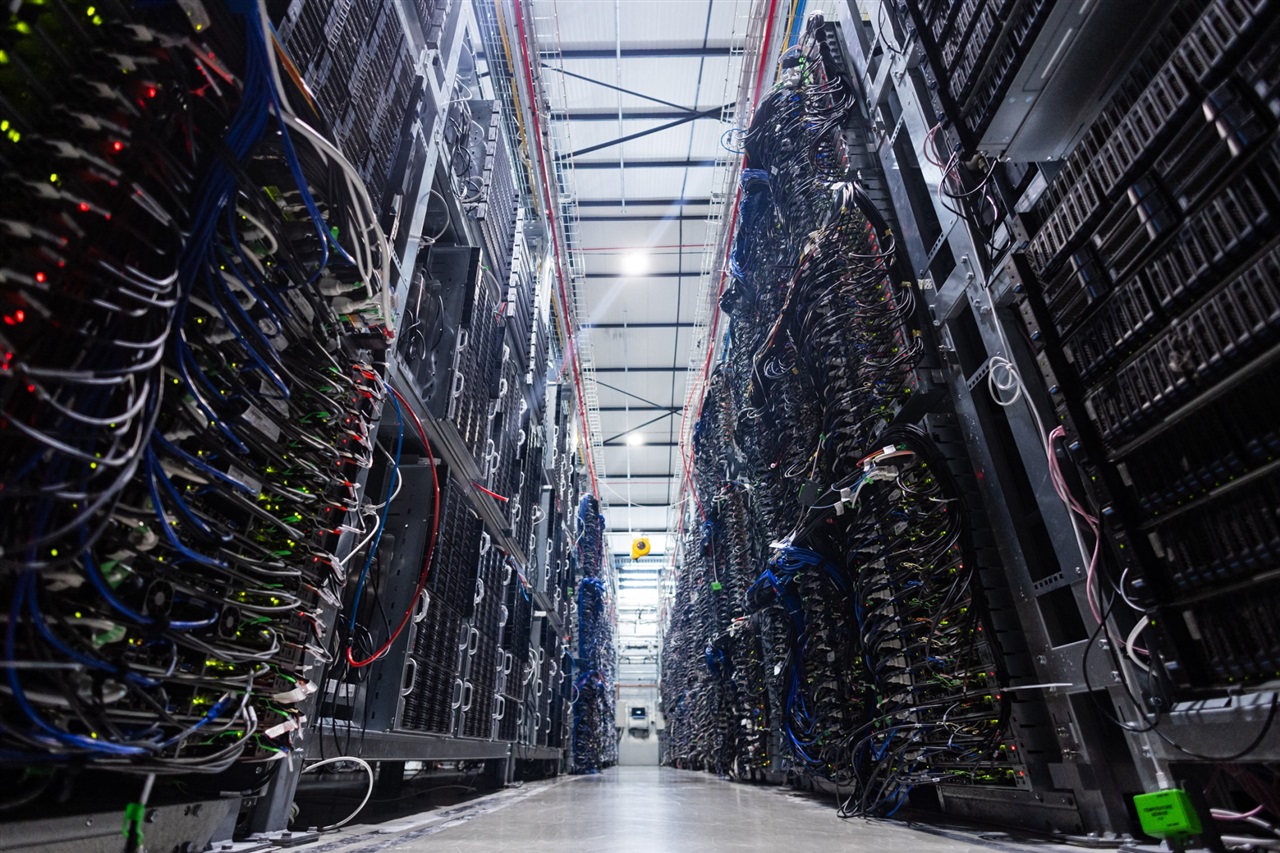
Training or running large AI models requires moving enormous amounts of data — model parameters, activation values, attention matrices — with extreme speed. A modern language model inference run on a 70-billion-parameter model requires moving hundreds of gigabytes per second just to load the weights into compute. The physics are unforgiving: compute scaling has consistently outpaced memory bandwidth improvements for decades, creating what engineers call the memory wall.
High-Bandwidth Memory stacks multiple DRAM dies vertically on-package, achieving over 1.2 TB/s bandwidth — versus 80 GB/s for conventional off-package memory. Critical for loading large model weights at speed.
Proprietary chip-to-chip interconnects allow 72+ accelerators to share a unified memory pool, enabling models that far exceed single-chip memory. The interconnect fabric is now as strategically important as the chip itself.
Chip-on-Wafer-on-Substrate integration co-locates compute dies and memory stacks at wafer scale, reducing interposer distance and dramatically boosting effective bandwidth density for AI workloads.
Emerging architectures perform computation directly inside memory arrays, eliminating data movement for specific operations — with the potential for 100× efficiency gains on memory-bound AI inference workloads.
The Energy Equation: AI Compute's Collision With Power Infrastructure
The AI processor race has an inescapable physical constraint: electricity. Training frontier AI models consumes power on the order of small cities for weeks or months at a time. A single high-performance AI accelerator draws 500–700 watts. A cluster of 30,000 such chips requires 15–21 megawatts of continuous power plus cooling infrastructure drawing power proportional to the compute load.
International energy forecasters estimated in 2024 that data center electricity consumption would double by 2026, with AI workloads as the primary driver. The response has been unprecedented: more nuclear power purchase agreements were signed in the past two years than in the previous decade combined.
"The AI processor question is no longer whether to invest. It is whether organizations understand their hardware dependencies deeply enough to make sound strategic decisions. Most do not — and the gap is widening rapidly."
— Enterprise AI Infrastructure Survey, 2025How AI Processors Are Accelerating Research Domains
The impact of faster AI compute is not abstract. Across multiple scientific and commercial domains, new processor generations have directly compressed timelines and enabled capabilities that were computationally infeasible at previous performance levels.
-
→
Drug Discovery and Molecular Biology
Protein structure prediction — once requiring years of experimental work per target — now runs in minutes to hours on AI processors, with accuracy matching experimental methods. This has unlocked rapid screening of millions of candidate molecules, compressing drug development timelines from decades to years for certain drug classes.
-
→
Climate Modeling and Weather Forecasting
AI weather models running on modern accelerators now produce medium-range forecasts in seconds versus hours for traditional numerical models. This speed advantage enables ensemble forecasting at scales previously impossible, improving the probability estimates that emergency planners depend on.
-
→
Software Engineering and Code Generation
The ability to train large code-specialized models and run them at low latency in developer tools has directly transformed software productivity. AI coding assistants running on inference-optimized hardware generate, review, and explain code in real time — only economically viable with the current generation of AI processors.
-
→
Materials Science and Clean Energy
AI models trained on materials databases can now predict properties of novel compounds and narrow the experimental search space by orders of magnitude, directly accelerating clean energy research — from high-efficiency solar cells to longer-lived batteries and lighter structural materials.
Strategic Implications: Five Decisions Technology Leaders Cannot Defer
- 01
Training vs. Inference: Where Is Your Compute Budget Going?
Most organizations use AI models rather than train them. Inference-optimized hardware often dramatically outperforms general-purpose accelerators on cost-per-query. Organizations that default to training-class hardware for all AI workloads may be substantially overpaying for production inference at scale.
- 02
Cloud vs. On-Premise: The Economics Are Shifting
Cloud GPU pricing has been elevated by unprecedented demand. For organizations with stable, predictable AI workloads at scale, owned or co-located hardware is increasingly competitive on total cost of ownership. The crossover point has moved significantly lower as hardware availability has improved.
- 03
Vendor Concentration: Is Your Infrastructure Over-Indexed on One Ecosystem?
Dominant software ecosystems create real developer advantages — but also significant supply chain dependency and pricing leverage. Investment in ecosystem-agnostic frameworks and pilot deployments on alternative hardware creates optionality that will matter as the competitive landscape develops.
- 04
Model Efficiency: A Better Model Often Beats More Hardware
Quantization, pruning, distillation, and mixture-of-experts architectures can reduce compute required to run a model by 50–90% with minimal performance degradation. Before purchasing additional hardware, organizations should audit whether their deployed models are running at appropriate precision and scale for the task.
- 05
Geopolitical Supply Chain Risk
Every leading-edge AI processor depends on fabrication capacity concentrated in a few geographic locations. Mature technology organizations are beginning to factor geographic supply chain risk into resilience planning in ways that go well beyond standard vendor risk assessment.
"The chip is no longer merely a component in an AI system. It is the strategic variable that sets the performance ceiling, defines the economics, and determines which organizations can reach capabilities that others cannot."
— Global Semiconductor Strategy Report, 2025What is certain is that the competitive stakes will not diminish. The organizations with access to the most capable AI silicon will hold structural advantages in every domain where artificial intelligence creates value: scientific discovery, software development, logistics, healthcare, defense, and financial systems. Understanding the processor revolution is no longer optional for anyone who wants to understand what comes next.